In a groundbreaking achievement, scientists from MIT, along with their collaborators, have successfully mapped the three-dimensional atomic structure of a relaxor ferroelectric for the first time. Their findings, which will be published in Science, lay a vital groundwork for enhancing models aimed at developing future computing systems, energy devices, and sophisticated sensors.
"With this newfound understanding, we can better predict and engineer the properties we desire in materials," stated James LeBeau, the Kyocera Professor of Materials Science and Engineering at MIT. "The research community is still refining methods to engineer these materials, but knowing whether our models are accurate is crucial for predicting their properties."
Uncovering Charge Distribution in Complex Materials
The research team employed an innovative imaging technique to analyze the distribution of electric charges within the material, leading to revelations that challenged prior assumptions.
"We discovered that the chemical disorder we observed was not fully accounted for in earlier studies," explained co-first authors Michael Xu and Menglin Zhu, both postdoctoral researchers at MIT. "By collaborating with our colleagues, we merged experimental data with simulations to enhance the accuracy of our models."
The study also included contributions from Colin Gilgenbach and Bridget R. Denzer, PhD students at MIT; Yubo Qi from the University of Alabama at Birmingham; Jieun Kim from the Korea Advanced Institute of Science and Technology; Jiahao Zhang, a former PhD student at the University of Pennsylvania; Lane W. Martin from Rice University; and Andrew M. Rappe from the University of Pennsylvania.
Investigating Disordered Materials at the Atomic Level
Previous computer models indicated that applying an electric field to relaxor ferroelectrics induces interactions between charged atoms, which contribute to their impressive energy storage and sensing capabilities. However, direct observation of these nanoscale regions had been elusive.
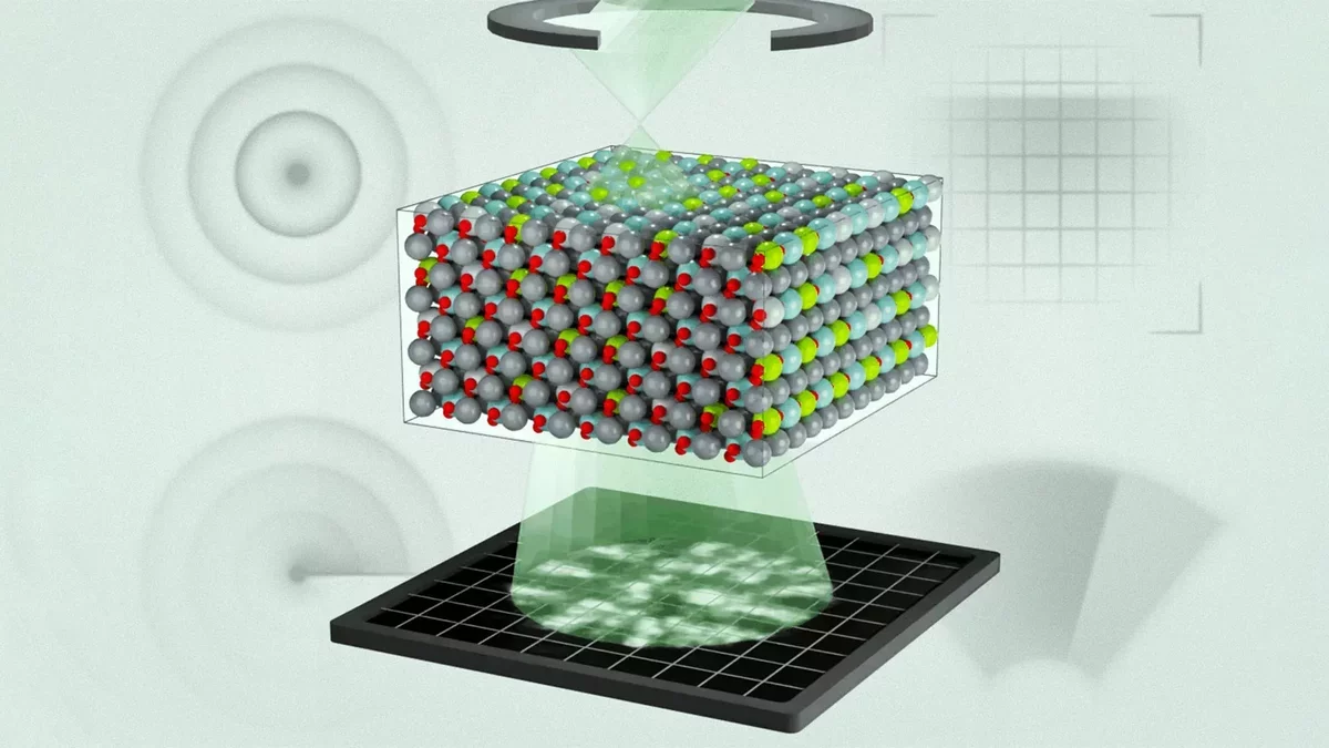
The researchers concentrated on a widely utilized material in sensors and actuators, a lead magnesium niobate-lead titanate alloy. They implemented a sophisticated technique known as multi-slice electron ptychography (MEP), which involves scanning a nanoscale beam of high-energy electrons across the material and capturing the resulting diffraction patterns.
"We sequentially acquire diffraction patterns at each position, creating overlapping regions that provide enough data for algorithms to reconstruct three-dimensional information about the material," Zhu elaborated.
This method revealed a complex hierarchy of chemical and polar structures, ranging from individual atoms to larger mesoscopic features. The team found that regions with varying polarization were significantly smaller than previously predicted by simulations. By integrating these observations into their models, they improved the accuracy of simulations in aligning with real-world behavior.
"Earlier models treated polarization regions randomly, lacking correlation insights," Xu noted. "Now, we can reveal how individual chemical species influence polarization based on the charge state of atoms."
Advancing Material Design for Future Technologies
Zhu emphasized the potential of electron ptychography in exploring complex materials, paving the way for new research avenues. "This study marks the first instance where we have directly linked the three-dimensional polar structure of relaxor ferroelectrics with molecular dynamics calculations," Xu remarked, underscoring the technique's capability to extract three-dimensional information from samples.
The team is optimistic that this approach will aid scientists in designing materials with customized electronic properties, enhancing technologies like memory storage, sensing systems, and energy devices. "As AI and computational tools evolve, materials science is increasingly embracing complexity in material design," LeBeau concluded. "Understanding the behavior of materials and validating our models is essential for future advancements."
The research received support from the U.S. Army Research Laboratory, the U.S. Office of Naval Research, the U.S. Department of War, and a National Science Graduate Fellowship, utilizing MIT.nano facilities.