A groundbreaking imaging technique, developed through a collaboration between Taiwan Semiconductor Manufacturing Company (TSMC) and Advanced Semiconductor Materials (ASM), has opened new avenues for understanding the atomic structures within computer chips. This innovation is poised to impact a wide range of technologies, from smartphones to quantum computers.
The findings, published in Nature Communications, feature doctoral student Shake Karapetyan as the lead author. David Muller, the Samuel B. Eckert Professor of Engineering at Cornell University, emphasized the significance of this technique for identifying defects during the development phase of computer chips.
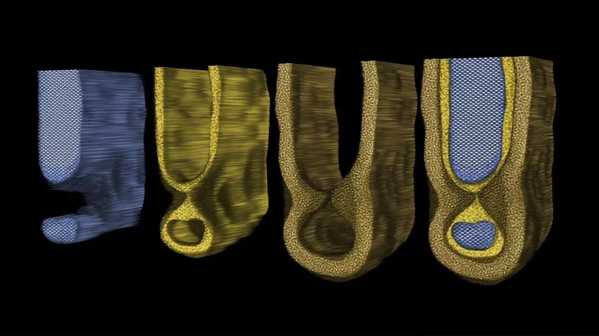
The Importance of Defect Detection
As semiconductor technology evolves, tiny structural flaws have become increasingly problematic. The complexity of modern chips means that even the smallest imperfections can significantly affect device performance. At the heart of each chip lies the transistor, a minuscule switch that regulates electrical current. Each transistor's channel must be meticulously crafted to ensure optimal electron flow.
"Think of the transistor as a tiny pipe for electrons," Muller explained. "If the pipe's walls are uneven, it can impede flow. Understanding the condition of these walls is essential."
Evolution of Transistor Design
Muller's extensive research into semiconductor limits dates back to his tenure at Bell Labs, where he explored the miniaturization of transistors. Initially, transistors were laid out flat, but as space became limited, engineers began stacking them vertically, creating intricate three-dimensional structures.
Today, advanced chips can host billions of transistors, with channels measuring only 15 to 18 atoms wide. This miniaturization makes diagnosing performance issues increasingly challenging, as even a single misplaced atom can impact functionality.
Advancements in Electron Microscopy
Throughout his career, Muller has collaborated with fellow scientist Glen Wilk to enhance electron microscopy techniques. Their previous work on replacing silicon dioxide with hafnium oxide has become foundational in modern processors. The latest development, known as electron ptychography, utilizes advanced electron microscopy to capture unprecedentedly detailed images of atomic structures.
This technique enables researchers to visualize the finest details of transistors, allowing for the identification of defects characterized as "mouse bites," which occur during the manufacturing process.
Future Implications
The ability to observe atomic-level defects has far-reaching implications for devices reliant on advanced chips, including smartphones and data centers. It also holds promise for the development of quantum computing technologies, which demand precise material control.
"This tool opens up new possibilities for scientific exploration and engineering control," Karapetyan noted. The study's co-authors include Steven Zeltmann from the Platform for the Accelerated Realization, Analysis and Discovery of Interface Materials (PARADIM), as well as Ta-Kun Chen and Vincent Hou from TSMC. This research was supported by TSMC, with additional funding for microscopy facilities provided by the National Science Foundation.